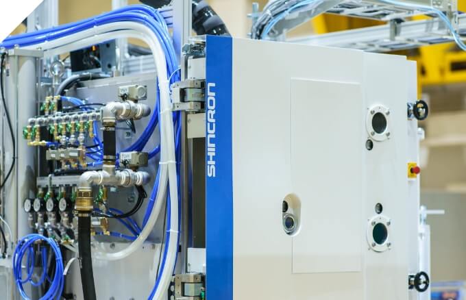


Cluster type single wafer sputtering system application
Cluster type single wafer sputtering system application: semiconductor, electronic and PIC markets
- Application:
- Electron and electricity control
Features
- High-quality deposition of crystalline thin films under a low-temperature process
- Capability of film deposition at optimal cathode position and angle based on deposition conditions and material characteristics
- Effective mass production by a C-to-C cluster tool
Major applications
- Deposition of functional thin films related to high-frequency filters and MEMS
- Crystal-oriented films
Piezoelectric materials / optical functional materials / metallic electrodes and so on - Film deposition related to PIC device
Low roughness, High-quality crystalline thin film deposition, High-oriented film deposition
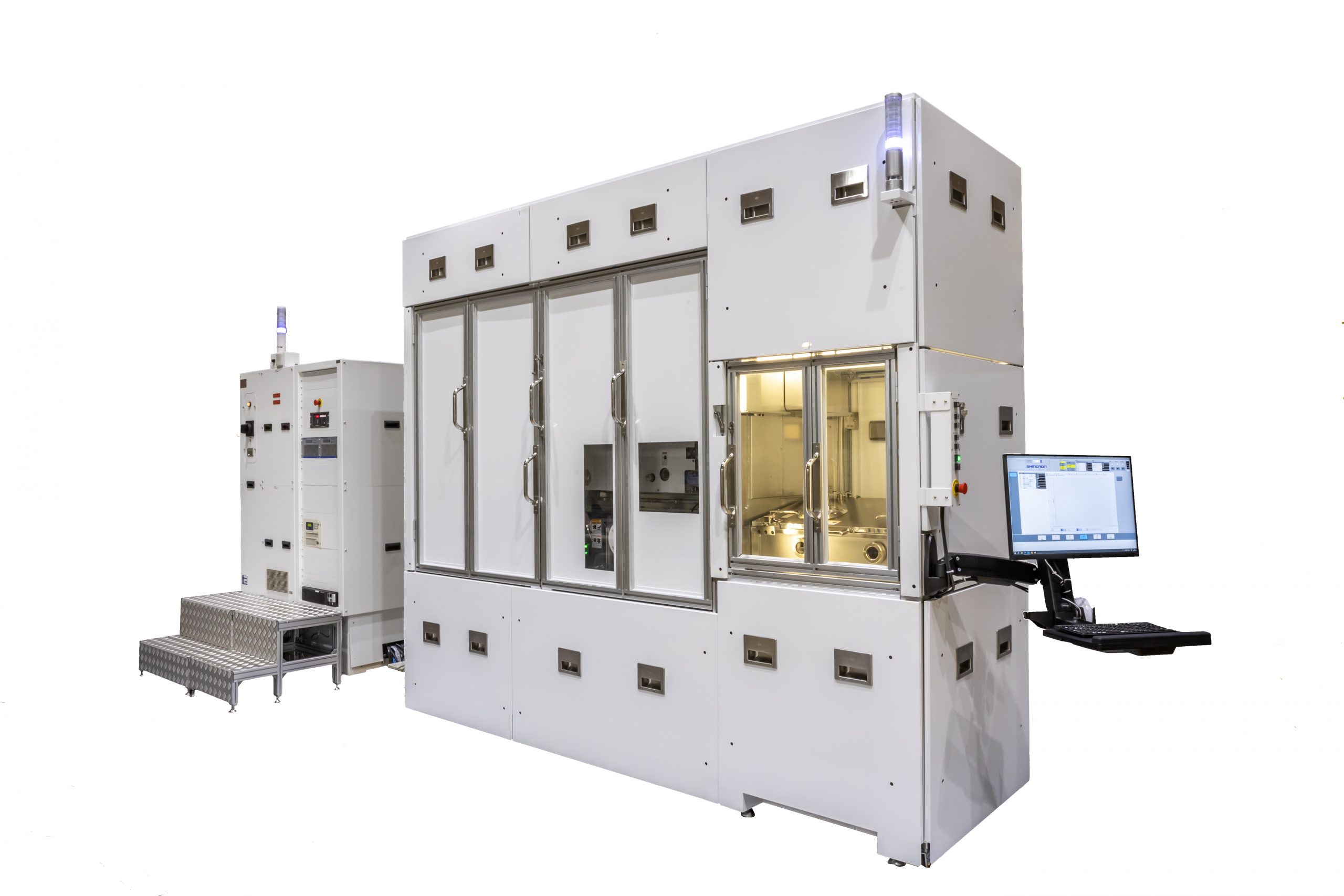
Specification outline
| Load lock chamber | -Wafer stage |
|---|---|
| Transfer chamber | – Vacuum wafer transfer robot |
| Sputtering chamber (Four chambers are connected as standard) |
– Circular fully-eroded cathode (⌀ 8” target) – Downward sputtering method |
| – Wafer heating mechanism (up to 600°C) – Substrate bias mechanism |
|
| – Power source for sputtering: RF (13.56 MHz)/DC – Power source for bias: RF (13.56 MHz) / DC * RF superimposed DC is applicable |
|
| – Exhaust system: TMP x 1 ultralow-temperature trap, dry pump – Ultimate vacuum < 2.0 x 10⁻⁵ |
|
| – SEMI/GEM-compliant interface |
Contact
We propose systems that meet
your requirements for functions
and applications.
Please feel free to contact us.
your requirements for functions
and applications.
Please feel free to contact us.
Sales Department
* Product specifications are subject to change for performance improvement without prior notice. For details, please contact our sales representatives.