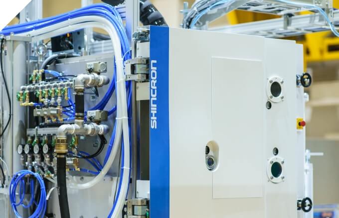


Cluster type RAS method-based film sputtering system for the semiconductor and electronic markets
A C-to-C handling-applicable cluster type RAS method-based film deposition system suitable for the semiconductor and electronics markets
- Application:
- Electron and electricity control
Features
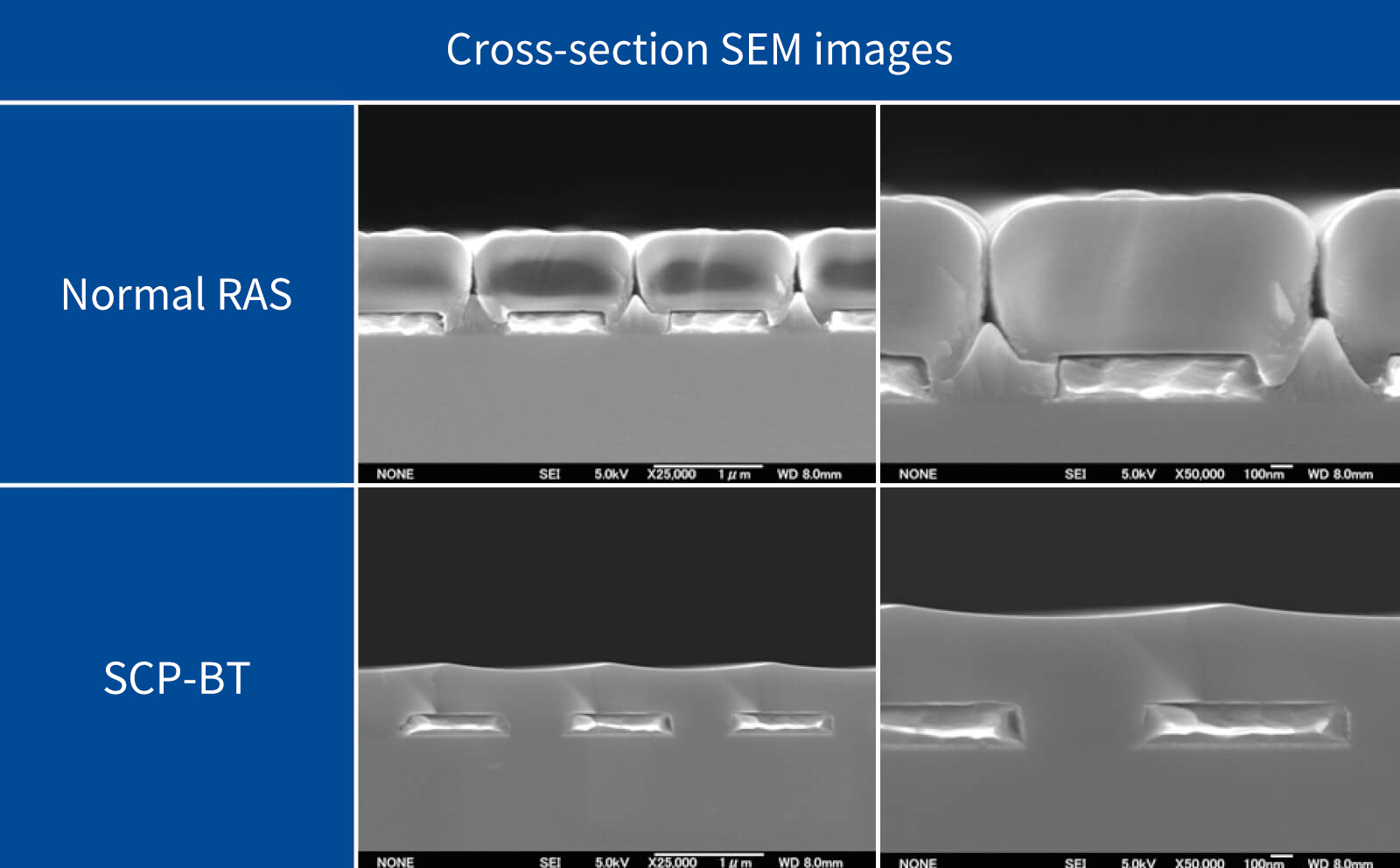
- Achieves the deposition of dielectric films at high throughputs using the load lock structure
- Enables step coverage by bias
- C-to-C handling suitable for wafer handling
- Enables overall film deposition on 8” substrates
Cooperation: Professor Hashimoto of Chiba University
Major applications
- SiO2 step covering/filling film deposition
- TC (Temperature Compensated)
- SAW temperature compensating films - Overall film deposition at high densities and low roughness
- Wafer bonding
- Various passivation films of SiO2 and SiN - Dielectric multi-layer films
- Acoustic multi-layer films for SMRs (Solid Mounted Resonators)
- Optical thin films for LEDs and LDs (Laser Diodes)
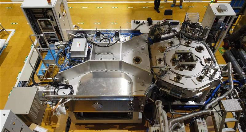
Specification outline
| Load lock chamber | – Wafer cassette station |
|---|---|
| Transfer chamber | – Vacuum wafer transfer robot – Aligner |
| Sputtering chamber (Up to two chambers can be connected) |
– Dual cathode (⌀ 12”) |
| – ICP plasma source – Substrate bias mechanism |
|
| – Rotary substrate stage (⌀ 6” x 25 pcs, ⌀ 8” x 20 pcs) | |
| – Exhaust system: 14” TMP x 2, ultralow-temperature trap, dry pump | |
| – SEMI/GEM-compliant interface |
Contact
We propose systems that meet
your requirements for functions
and applications.
Please feel free to contact us.
your requirements for functions
and applications.
Please feel free to contact us.
Sales Department
* Product specifications are subject to change for performance improvement without prior notice. For details, please contact our sales representatives.