

10. Points for thin film deposition
10.1 Growth processes and structures of thin films
What kind of process is undergone when substances are evaporated in a vacuum to form a thin film on a substrate? Firstly, it is known that there are three types of early processes, as shown in Figure 10.1.
- Core growth type (Volmer-Weber mode): The cores generated on a substrate grow up and become integrated with each other to form a thin film. Most thin films are formed in the process like this.
- Single-layer growth type (Frank-von der Merwe mode): Atoms that form a thin film cover a substrate surface uniformly to form atomic monolayers sequentially. This type of growth is observed in PbSe/PbS, Au/Pd, and Fe/Cu.
- Complex type (Stranski-Krastanov mode): A core growth occurs after one or two atomic monolayers are formed first. This type of growth is likely to occur when depositing metals on clean metallic surfaces, and Cd/W, Cd/Ge, and so on belong to this type.
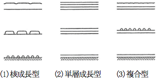
Figure 10.1 The three types of thin film growths 1)
The type of thin film growth is estimated to depend on the cohesive force of thin film substances, magnitude relation of adsorption force between a thin film and a substrate, substrate temperature, and so on.
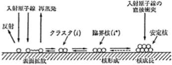
Figure 10.2 The formation and growth of cores on a substrate 1)
Figure 10.2 describes the core growth type thin film forming process.
- Among the thin film substances that collided with a substrate, some are reflected and others are adsorbed
- The adsorbed atoms diffuse on the substrate surface to form clusters as a result of a two-dimensional collision between the atoms or re-evaporate after staying on the surface for a certain amount of time
- The clusters continue colliding with the atoms diffusing on the surface or releasing single atoms, but they become stable cores after the number of atoms exceeds a certain critical level
- The stable cores continue growing by capturing the atoms diffusing on the surface and colliding directly with incident atoms
- The stable cores continue growing and are coupled with neighboring stable cores (coalescence) to finally form a continuous film
The structure of a thin film whose thickness has reached a certain degree varies depending on the film forming method and condition. As an example, Figure 10.3 shows the Thornton model that is famous in the sputtering field.
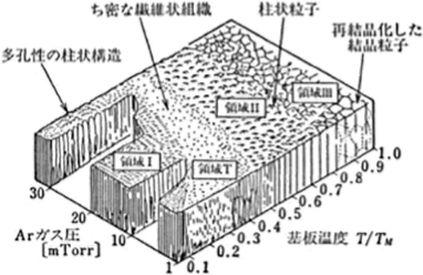
Figure 10.3 Thornton model 2)
10.2 The definition of and measuring method for film thickness
When evaluating a thin film, it is very important to determine its film thickness. On the other hand, however, it is also important to understand the essence of the measuring method before conducting a measurement. For details, please refer to the detailed explanation given in reference 3). Here, the definition of film thickness is described.3)
- Shape film thickness (Geometric film thickness)
It refers to the distance between the average surface of a thin film and the average surface of a substrate.
Major measuring methods include step measurement using a stylus type surface roughness meter and measurement based on the observation of film shape with an electronic microscope. - Mass film thickness
It refers to the distance between the average surface of a thin film and the average value of a substrate surface, when the thin film mass is rearranged in a way such that its density becomes equivalent to that of bulk (a lump state) and placed uniformly on the substrate surface.
Measuring the number of atoms using fluorescent X-rays is also one of the methods of measuring mass film thickness. - Physical property film thickness
It refers to the distance between the average surface of a bulk substance, which shows the same value as the bulk formed on substrate surface uniformly when the physical properties of a thin film are measured, and the average value of the substrate surface.
The measured properties include electrical properties such as electric resistance and capacitance as well as optical properties such as reflection rate and transmittance.
For example, in the case of an optical thin film, physical film thickness refers to a value calculated by dividing the value of optical film thickness obtained from the spectroscopic characteristics (the product of the refractive index and the shape film thickness) by the refractive index, assuming that this thin film has uniformly the same refractive index.
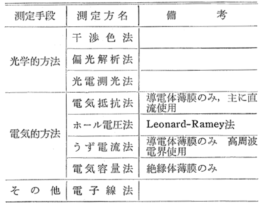
Tables 1, 2, and 3 show the film thicknesses and the methods of measuring them cited from reference 3).
Table 1 Shape film thickness measuring method
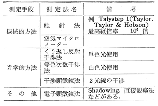
Table 2 Mass film thickness measuring method
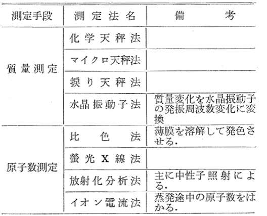
Table 3 Physical film thickness measuring method
10.3 Problems in the formation of thin films
Even if a thin film, which is attempted to be formed, is found experimentally to satisfy the required properties, the following problems need to be studied considering its reproducibility and productivity:
- Film thickness control technology
- Film thickness determination method
What film thickness and how should it be measured to determine the properties required for the thin film to be formed?
Generally, optical type film thickness gauges are used for optical thin films and quartz type film thickness gauges are used for other types of thin films. - Control of film forming velocity
What kind of monitor should be used and how should the film forming velocity be controlled?
The methods that control the power of evaporation, sputtering, and plasma sources by giving feedback from a quartz type film thickness gauge are frequently used. - Film thickness distribution
How much film thickness distribution (and distribution of other properties) is required?
What kind of system configuration should be chosen and how should the film thickness distribution be corrected in order to realize the desired film thickness distribution?
In deposition-based film forming methods, the film thickness distribution can be corrected using a film thickness correcting plate. However, in the case of sputtering and CVD, the method is dependent on the system configuration.
- Film thickness determination method
- Adhesion
In situations where a thin film is used, whether it has sufficient force to adhere to a substrate or not is an important problem. The matters that should be considered in order to achieve the required adhesion are as follows:- Combination of film type and substrate
- Cleaning of substrate (process, cleaning agent, drying method, and so on)
- Pre-treatment of substrate (such as ion irradiation)
- Film forming conditions
- Time-dependent change of adhesion
- Internal stress
The internal stresses generated in thin films include the followings:- Thermal stress
It is generated by the difference in thermal expansion coefficient between a thin film and a substrate (a bimetallic effect). - True stress
- Surface effect
– Surface tension: Dominant in the early phase of thin film formation.
– Surface layer: Because of the formation of an oxidation layer, and so on.
– Crystal grain boundary: Generated in the process of binding and growth of island-like crystals. - Volume effect
– Phase transition: From amorphous to crystal and liquid phase
-> Because of a change in volume associated with a transition of phase to the solid phase, and so on.
- Surface effect
- Thermal stress
- Film strength and density
Compared to bulks, thin films have lower densities and strengths. Except for special applications, realizing thin films as close to bulks as possible is the goal of the thin film forming technology. To achieve this, various new technologies have been developed.
Aside from this, the film strength decreases temporarily to generate defective films. In most of such cases, the film forming systems have a problem, so they need inspection.
The most common problem is dirt inside the film forming chamber. Film materials adhere to the internal wall of the film forming chamber, in addition to substrates. Additionally, the materials form a thick film if they adhere repeatedly. In particular, in the case of batch type systems whose film forming chamber is exposed to atmosphere and put under vacuum repetitively, the thin film adhering to the areas other than substrates becomes a porous one with very low density and many void spaces, compared to thin films adhering to substrates.
As this porous thin film has a large surface area, it absorbs a large amount of water in the atmosphere when it is exposed to the atmosphere. Then, this water is released into a vacuum while the next film is formed.
An important factor for achieving film density and strength that are close to those of bulk is the ratio of film substances and impurity gases during film formation. The higher the rate of the film substances is, the closer to bulks the thin films become.
If a film is formed when the film forming chamber is dirty inside, a large amount of water adsorbed to the dirt is released and stays near a substrate. In other words, the rate of impurity gases increases, and a thin film with low density and strength is formed. To prevent this, cleaning the vacuum chamber in a periodical and planned manner is important. Generally, in film forming systems, a stainless-steel adhesion prevention shield plate can be mounted to simplify the cleaning operation. Therefore, a dirty shied plate is replaced with a spare shield plate and cleaned with a sandblast system to be ready for the next replacement.
In addition, the film density and strength also decrease temporarily when a vacuum leakage occurs. By maintaining film forming systems daily, most unexpected problems can be avoided. - Pinhole and particle
Particularly in the semiconductor industry, tiny pinholes and particles that had not been problems are becoming problems due to recent miniaturization of patterns. The first important point to reduce them is to keep substrates clean at all times.
In addition to the control and cleaning of clean rooms as well as measures taken in the pre-treatment process, attention also needs to be paid to dirt on the inner wall of film forming systems. In addition, a description is given about particles in the next section again, because a major cause of the particles is a large block of thin film substances that scatter before they are evaporated. - Problems with systems
- Vacuum exhaust system
Suitable types of vacuum exhaust systems vary depending on the properties required for thin films and substrate types.
For example, in the case of resin substrates, it is effective to use cryopumps or Meissner traps whose water discharge velocity is high, because a large amount of water (H2O) is discharged when gas is exhausted to create a vacuum.
Oil-sealed rotary pumps and diffusion pumps have many advantages such as less frequency of failure and lower prices. On the other hand, however, a small amount of oil flows back into the vacuum chamber in these pumps. As a result, this could be a cause of the generation of pin holes if elements with fine patterns are used. In such a case, it is preferable to use an oil-free exhaust pump, and using a dry pump as a roughing pump as well as a cryopump or turbo molecular pump as a high vacuum pump is recommended.
In addition, improper use of an oil-sealed rotary pump has caused a significant backflow of oil in many cases. This is because the roughing time was longer than necessary. If gas is exhausted under a pressure of several pascals or lower using an oil-sealed rotary pump for long hours continuously, a significant amount of oil flows back into the vacuum chamber. As countermeasures, minimizing the roughing time, exhausting gas with a high vacuum pump, or mounting an oil trap into the roughing pipe is recommended.
Dust attached to substrates could cause pinholes when they desorb, and could cause a problem as a huge particle when they remain in the film in the case of substrates with fine patterns. In most cases, dust is generated from the thin film substances adhered to the inner wall of the vacuum chamber or jigs, when they adhere to the substrates after coming off and being flung up at the initiation of exhaustion or at the time of vacuum break. To prevent this, adopting slow gas exhaustion and slow leak, in which the gas exhaustion is started and the gas is leaked slowly, is effective. - Vacuum chamber and internal mechanism
In film forming systems, dust and gases generated in and released from the internal mechanism such as vacuum chamber, jigs, and transferring mechanism affect the characteristics of thin films significantly.
As the substrate holder is located closest to the substrates, minimizing the dust generation and gas release from the substrate holder is a point for forming high quality films. Specifically, dust generation can be reduced by sandblasting the adhesion prevention shield plate, to which unnecessary thin film substances adhere, to prevent the adhered substances from coming off. In addition, be careful when forming films through heating film deposition using a substrate jig made of Zn that is an easy-to-process material, because it may contaminate thin films as well as exhaust systems.
It is desirable that no oil is applied to the bearings employed in the transferring mechanism. However, if there is no choice but to use oil, using a minimum amount of oil with low vapor pressure is important. - Evaporation and sputtering sources
As mentioned earlier, relatively large particles in thin films have been becoming a problem in many cases due to the miniaturization of patterns.
In evaporation sources, evaporation materials may be splashed because of dust, and large particles may adhere to substrates. To prevent this, the following measures can be taken:
1. Increase the purities of evaporation materials and decrease the occluded gases
2. Improve the shapes of evaporation materials
3. Heat the evaporation materials sufficiently and preliminarily, and degas them
Also in sputtering sources, the same measures as the ones taken for the evaporation materials need to be taken for the target materials. As an important measure, the generation of particles caused by an abnormal electrical discharge due to the charge-up of charged particles on the target surface needs to be prevented.
- Vacuum exhaust system
10.4 References
- Edited by the 131st committee of Japan Society for the Promotion of Science, Thin Film Handbook, page 64, Ohmsha, Ltd. (1983)
- J. A. Thornton, J. Vac. Sci. Technol, 11, 666 (1974)
- Akira Kinbara, Method of Measuring the Thickness of Vapor-Deposited Thin Films (1), Vacuum, Vol. 11, No. 10 (1968)