

9. Examples and applications of films formed with Shincron’s film forming systems
Shincron has developed systems to respond to strict user requirements since its foundation in 1951. From among its systems, the characteristic ones are described below.
9.1 Continuous systems
In continuous systems, the processing chamber and the loading/unloading chamber are separated by a gate valve so that the processing chamber is not exposed to atmosphere and a high vacuum is maintained. Therefore, continuous systems have the following features:
- Stable film forming process
- Shortened film forming process
Shortened time before reaching the pressure at which film formation is started
In particular, CES can realize a very efficient process, if the gas exhaustion, heating treatment, and film formation times are in the same process. - Reduced particles
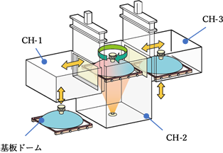
In addition, as Figure 9.1 (a) shows, the CES-2M and 3M models are characterized by the saving of space in a clean room, because the entire system does not need to be placed in a clean room.
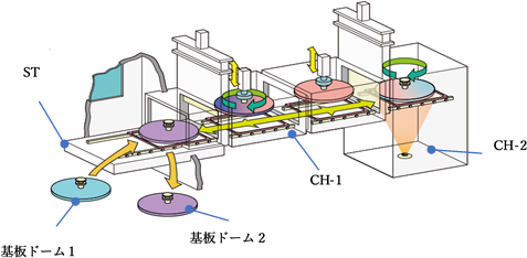
(a) CES-2M model 5)
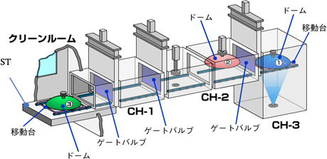
(b) CES-3M model 1)
(c) CES-D model
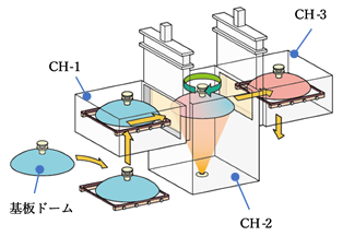
(d) CES-S model
Figure 9.1 The schematic diagrams of respective models of CES system 1)
The roles of respective CHs in each model of CES system are as described below.
| (a) CES-2M model | ST: | Places a substrate dome on the transfer table (mechanism). |
|---|---|---|
| CH-1: | Loading/unloading – Heating treatment/gradual cooling treatment – Exhausts atmosphere to create a vacuum and release the vacuum to return to atmosphere. – The mechanism that travels back and forth between ST, CH-1, and CH-2 is located in the lower position. – Moves a substrate dome before film formation from ST to the upper position of CH-2. – Moves a substrate dome after film formation to the lower position of CH-2 and from CH-2 to the lower position of CH-1. – Moves a substrate dome before film formation from CH-1 to CH-2. – Moves a substrate dome after film formation to the lower position, releases it to atmosphere, and moves it to ST |
|
| CH-2: | Implement the film forming process. – CH2 is constantly kept under high vacuum. – Keeps the necessary amount of film forming materials in stock and supplies them every time a layer is formed. |
|
| (b) CES-3M model | ST: | Places a substrate dome on the transfer table (mechanism). |
| CH-1: | Loading/unloading – Heating treatment/gradual cooling treatment |
|
| CH-2: | Transfer mechanism and post-treatment process – The transfer mechanism is the same as that of CES-2M – Performs additional post treatments that require vacuum, such as water repellent treatment, before moving from CH-2 to CH-1. |
|
| CH-3: | Implements the film forming process. | |
| (c) CES-D model | CH-1: | Loading/unloading Heating treatment/gradual cooling treatment |
| CH-2: | Film forming process | |
| CH-3: | Loading/unloading – Heating treatment/gradual cooling treatment |
|
| (d) CES-S model | CH-1: | Loading |
| CH-2: | Film forming process | |
| CH-3: | Unloading – Post-treatment process |
The CES model systems can be adapted to the installation layout of users and are widely used in the mass production of antireflection films for cameras, spectacles, and other optical components as well as optical thin films with up to approximately 20 layers.
9.2 EPD
EPD (Effective Physical Vapor Deposition) is a film forming method developed by evolving and expanding IAD and enables the formation of super multiple-layer films that cause less scattering. Figure 9.2 shows the conceptual diagram of EPD.
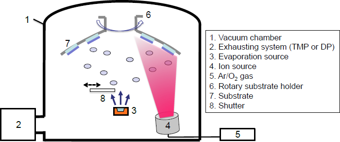
Figure 9.2 The conceptual diagram of EPD 2)
The effects that can be produced by irradiating a part of a substrate dome with high density ions during film formation are described as follows:
- Establishing a region that is irradiated with high density ions and a region that is not irradiated with the ions on a thin film to be formed makes the relaxation time during which the thin film formation becomes stable. As a result, migration is promoted in the thin film and a high density thin film is formed.
- Through irradiation with high density ions, the portions of the thin film with low density are etched and only the thin film with high density remains.
A super multi-layer film of TiO2/SiO2 with 282 layers and a total film thickness of 33 µm was formed through EPD. Figures 9.3 and 9.4 show an AFM image and a cross-sectional SEM image of its surface, respectively.
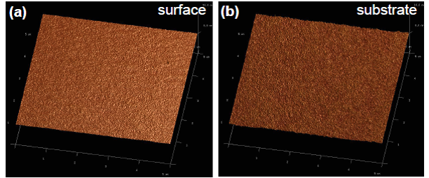
Figure 9.3 An AFM image of a super multi-layer film of TiO2/SiO2 with 282 layers and a total film thickness of 33 µm 2)
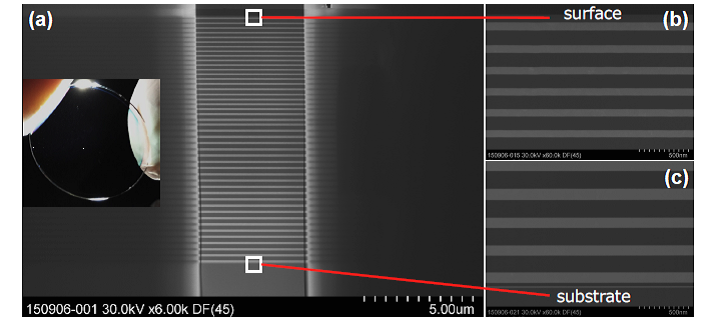
Figure 9.4 A cross-sectional SEM image of a super multi-layer film of TiO2/SiO2 with 282 layers and a total film thickness of 33 µm 2)
In the case of the IAD method, there is a tendency that the Haze value (equivalent to scattering) becomes low but stress increases when an ion current density is increased. As Figure 9.5 shows, it can be confirmed that the stress becomes low when a film is formed through EPD, even if the Haze value is at the same level. Therefore, EPD is expected to be applied to laser optical systems that require low loss and high Laser-Induced Damage Thresholds (LIDTs).
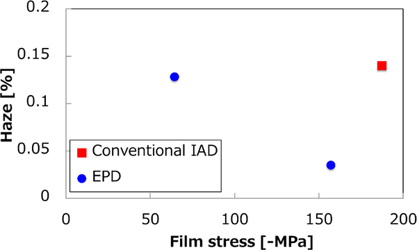
Figure 9.5 A comparison of the stress between the general IAD method and the EPD method 2)
9.3 RAS
Concerning the RAS method as previously mentioned in 5.2.5, the detailed features are described below.
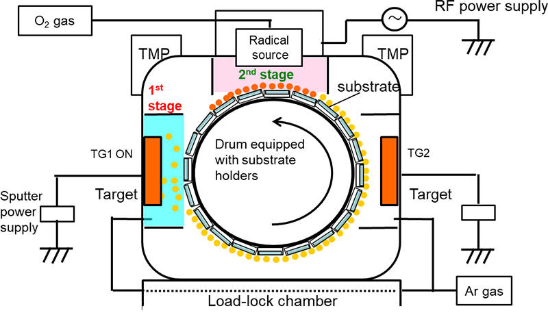
Figure 9.6 The outline of the RAS method 3)
The vacuum chamber consists of CH-1 that loads/unloads substrates and CH-2 that is equipped with a high vacuum exhaust system, target, and radical source.
9.3.1 Target section
Films are formed in a metallic mode region with high film forming rate, avoiding the hysteresis of reactive gases during reactive sputtering as shown in Figure 5.17. This prevents abnormal electrical discharge on a target surface, as shown in Figure 5.18. Figure 9.7 shows a photo of the surface of a Si target that was used at 40 kwh in the RAS-1100B system. Si target is a material used when forming a film of SiO2 that is an essential low refractive material for optical thin films. Abnormal electrical discharge occurs most frequently when forming SiO2 films through reactive sputtering, so SiO2 is a material that is difficult to form stably.
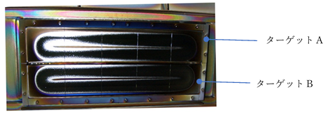
Figure 9.7 A photo of a Si target surface after it is used at 10 kwh in the RAS-1100B system 1)
With regard to the anode disappearance as described in Figure 5.18, the stability of electrical discharge is ensured by employing AC sputtering (dual cathode).
The principals of the measures against abnormal electrical discharge and anode disappearance through AC sputtering are as described below.
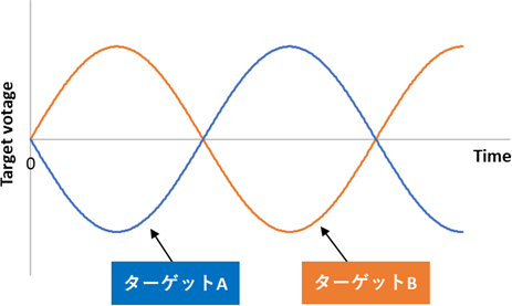
Figure 9.8 The time course of the voltages applied to the targets 1)
As a high voltage is applied to targets A and B alternately (between 40 and 100 kHz) as Figure 9.8 shows, a positive or negative voltage is constantly applied to the targets in each half cycle. The incomplete oxides accumulated on the target surfaces while a positive voltage is applied are sputtered when a negative voltage is applied so that clean metallic surfaces are constantly secured. In addition, an abnormal electrical discharge caused by ionic charges due to the incomplete oxides is neutralized by electrons when a positive voltage is applied, as shown in Figure 9.9.
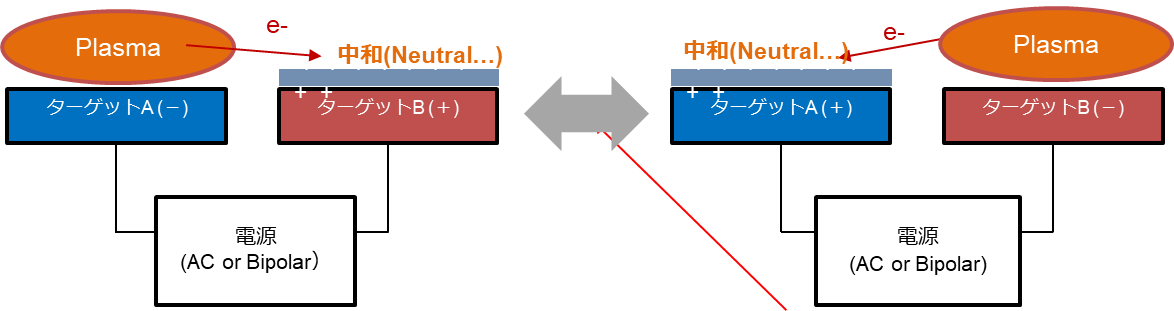
Figure 9.9 A strategy to prevent abnormal electric discharge from occurring at the targets 1)
9.3.2 Substrate temperature
Figure 9.10 shows a variation in substrate temperatures during the film formation through RAS. When an IR cutoff filter with a total film thickness of 3.8 µm was formed, the standard film forming time was 148 minutes and the substrate temperature rose from room temperature to approximately 170°C. On the other hand, however, under low temperature film forming conditions, the film forming time was longer but the substrate temperatures decreased to 106°C and 86°C. As long as the temperatures increase in this way, the RAS method is also applicable to resin substrates.
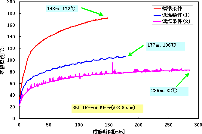
Figure 9.10 A variation in substrate temperatures during the film formation though RAS 3)
9.3.3 Film formation examples
1) Formation of mixed films
As Figure 9.6 shows, two pairs of targets are placed in the process chamber. This enables the process of forming a mixed film as shown in Figure 9.11. The composite metal mixing ratio can be varied freely by selecting a power ratio for respective pairs of targets.
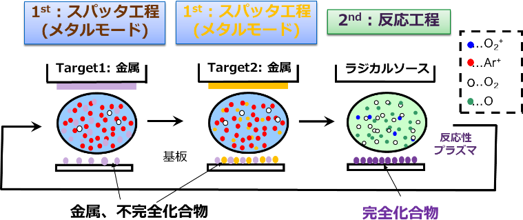
Figure 9.11 Formation of a film using two types of metal through RAS 3)
Figure 9.12 Preparation of intermediate refractive indexes achieved through RAS 3)
Although it had been known in the design of optical filters for a long time that an optical filter with superior properties could be obtained by using materials with three or more types of refractive indexes, it was difficult to actually form thin films with arbitrary refractive indexes. Therefore, two types of substances with high and low refractive indexes have been generally used in combination to design an equivalent film. RAS enables easy realization of intermediate refractive indexes as shown in Figure 9.12. By using intermediate refractive indexes, a PBS (Polarizing Beam Splitter) that can divide light into s-polarized light and p-polarized light even if the incidence angle changes significantly can be realized easily. Figure 9.13 shows an example of a formed film. It can be found that this film has superior spectral characteristics even if the incidence angle changes by +/- 12°.
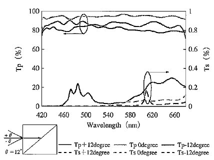
Figure 9.13 The spectral characteristics of a prism-type PBS formed using an intermediate refractive index at incidence angles of 0° and +/- 12° 3)
3) Various types of optical thin films
Figure 9.14 Broadband antireflection film (AR) 1)
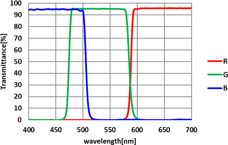
Figure 9.15 RGB filter 1)
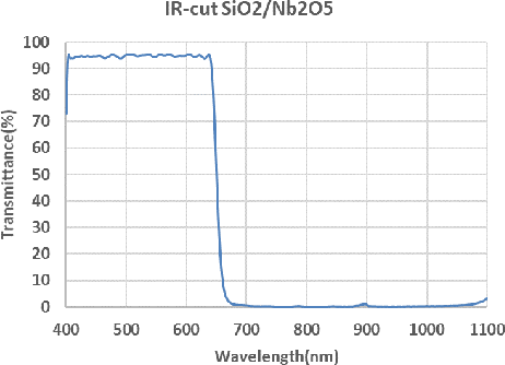
Figure 9.16 IR cutoff filter 1)
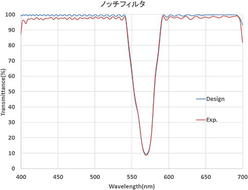
Figure 9.17 Notch filter (Minus filter) 1)

Figure 9.18 Bandpass filter 1)
9.4 SLS
SLS is a system developed by adapting and evolving the RAS method that is proven in the optical thin film field to the electronic component field
The points of evolution from a RAS-based system as a system for the electronic component field are as described below.
- Applicable to clean rooms
- Compatible with wafer loaders
- Formation of films with superior step coverage (covering a surface with bumps and dips of 100 nm with dielectrics)
As an application, the formation of SiO2 film using TC-SAWs (Temperature Compensated Surface Acoustic Waves)
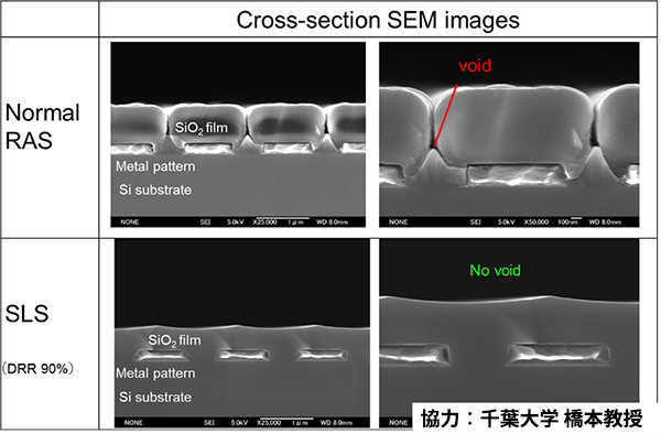
Figure 9.19 Improvement of step coverage by the SLS system 1)
9.5 P-RAS
P-RAS is a compact RAS system for research use that had been strongly requested.
Although the sputtering and reaction processes were spatially separated in the conventional RAS system, the sputtering film formation and reaction processes are separated in terms of time in the P-RAS system. Therefore, the P-RAS system is suitable for searching new materials.
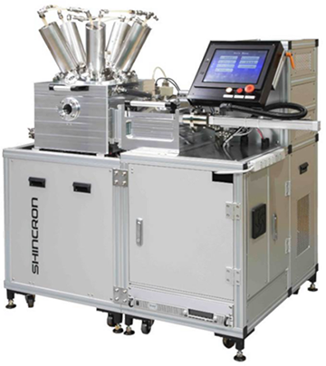
Figure 9.20 The external appearance of the P-RAS system 1)
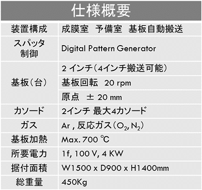
Table 9.1 The outline of the specifications of the P-RAS system 4)
Figures 9.91 and 9.22 show an SEM image and the performance of (Er0.1Y0.9)2Zr2O7 formed with a P-RAS system.
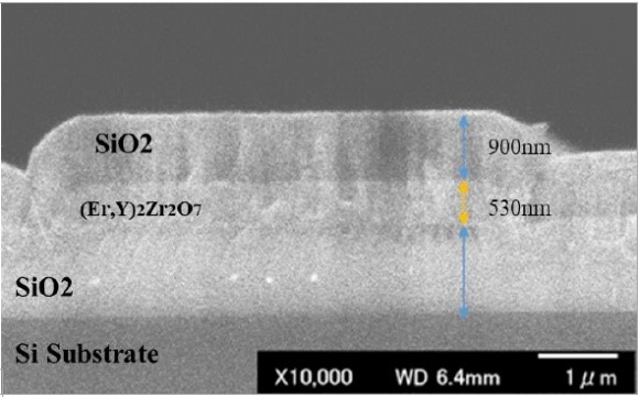
Figure 9.21 A cross-sectional SEM image of (Er0.1Y0.9)2Zr2O7 waveguide 4)
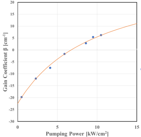
Figure 9.22 The optical gain property of (Er0.1Y0.9)2Zr2O7 waveguide as a function of the excitation 4)
9.6 PMC
The features of the PMC series systems as high-quality metallic electrode forming systems for electronic components represented by SAW are as described below.
The features of the PMC series systems are as follows:
- A structure with separated load lock chamber and film forming chamber
As the ultimate pressure is 10-5 Pa level, films can be constantly formed in a high vacuum of 10-5 Pa level - The film forming process is performed through deposition using an EB (Electron Beam)
A special hearth liner structure - A structure where an EB and a quartz type film thickness gauge are placed in the substrate rotation center
Using a system with the features as described above, the following film formation can be realized:
- Lift-off film formation
- Precise film thickness control
- Metallic thin films with low surface roughness
- Metallic thin films with a specific resistance similar to that of bulk
- Metallic thin films with uniform film thickness distribution (within batch and between batches)
- Alloy thin films with stable specific resistance
- Metallic thin films with high reflection rate
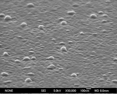
Al is a material that is commonly used as electrodes for electronic components. However, as it is very active and low in melting point, it is likely to get oxidized and form hillocks. Therefore, it is very difficult to form smooth surfaces. Below are the SEM images of the surfaces of Al thin films formed with a PMC system and a conventional system, respectively.
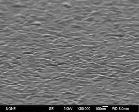
An Al thin film formed with a PMC system
R = 92% @ 400 nm, ρ = 2.86 µΩcm
A conventional Al thin film
R = 90.2% @ 400 nm, ρ = 3.3 µΩcm
Figure 9.23 A comparison of the SEM images of the surfaces of Al thin films formed with a PMC system and a conventional system 1)
In addition, current mobile terminals require small/high-power SAWs4), and the PMC system enables the formation of Al thin films with high orientation. Figure 9.24 shows the result of an XRD measurement of an Al thin film formed with a PMC system.
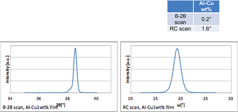
Figure 9.24 The measurement of the orientation of an Al thin film formed with a PMC system 1)
9.7 IBF(Ion Beam Figuring)
In recent years, there are increasing needs for the direct bonding of semiconductors, a combination of semiconductor and metal, a combination of semiconductor and glass, and so on in the fields of high-performance sensors, semiconductors, and electronic components. In addition, applications where product surfaces are processed through IBF have been expanding for the purpose of adjusting the frequencies of radio-frequency components, improving the surface roughness of high-resolution imaging lenses, and so on. For such applications, Shincron sells IBF systems in Japan as a distribution agent for Bühler Alzenau (Leybold Optics Business).
9.8 References
- Shincron Co., Ltd., catalogue
- M. Miyauchi, K. Okada, S. Ito, Y. Jiang, S. Samori, E. Nagae: Scatterless SiO2/TiO2 multi-layered thick UV-IR cut filter prepared by EPD system, Optical Interference Coatings (OIC) (2016)
- Ekishu Nagae, Sputtering Film Forming System for Optical MultiLayers, Vacuum Technology Outlook 2006, Electronic Journal (2006)
- Kodai Miyagi, Yasuhito Tanaka, Ayuko Minowa, Ghent Nakamura, and Hideo Isshiki, Optical Gain in Mid-Refractive Index Contrast (Er0.1Y0.9)2Zr2O7/SiO2 Waveguide Prepared by Radical Assisted Sputtering, Solid State Device and Materials (SSDM) 2019 (2019)
- Osamu Nakagawara, Masahiko Saeki, Masanobu Watanabe, Kazuhiro Inoue, Toshio Hagi, Takahiro Makino, Seiichi Arai: Epitaxially grown aluminum films with titanium intermediate layer on y rotated Y2X LiNbO3 piezoelectric single crystal substrates, Journal of Crystal Growth 249 (2003) 497–501
10. Points for forming thin films
- 1. Introduction
- 2. History of thin film deposition using vacuum
- 3. Basics of vacuum
- 4. Plasma
- 5. Various film deposition technologies based on the Physical Vapor Deposition (PVD) method
- 6. Actual PVD systems
- 7. Various film deposition technologies and systems based on the Chemical Vapor Deposition (CVD) method
- 8. Thin films created using vacuum
- 9. Examples and applications of films formed with Shincron's film forming systems
- 10. Points for thin film deposition
- 11. Maintenance of thin film deposition systems
- 12. Conclusion