
8. Thin films created using vacuum
Major fields of use of thin films formed utilizing a vacuum are described briefly below.
8.1 Optics
As long as optical components that utilize lights exist, optical thin film technology is essential for controlling the transmittance and reflection rate of light.
In recent years, the utilization of plasma in film forming processes has become widespread, by increasing the densities and stabilizing the refractive indexes of dielectrics that are the constitutional materials for optical films. This is because optical components can be utilized more stably through adding a performance for achieving less wavelength shift (a phenomenon where moisture in the environment is incorporated into a thin film, varying the refractive index and optical properties) to optical films.
For optical components that utilize light, optical thin film technology is essential for controlling the transmittance and reflection rate of light.
In recent years, the utilization of plasma in film forming processes has become widespread in order to increase the densities and stabilize the refractive indexes of optical thin films.
In conventional film forming methods (that do not use plasma), a phenomenon occurred where moisture in the environment was incorporated into thin films, varying the refractive indexes and optical properties. This phenomenon is called wavelength shift. Using plasma enabled an increase in the filling densities of thin films and the prevention of wavelength shifts. In addition, as the refractive indexes of thin films became stable, it became possible to form films with high reproducibility.
8.1.1 Antireflection film
Antireflection film is a typical optical thin film and consists of multi-layer dielectric thin films. This film is mainly formed by the IAD and RAS methods. Additionally, as its constitutional materials, MgF2 is used for fluoride films, and SiO2, ZrO2, Al2O3, TiO2, and Ta2O5 are used for oxide films.
Antireflection films usually consist of a single layer or 3 to 7 layers of MgF2. However, the importance of antireflection films increased in association with Virtual Reality (VR), Augmented Virtuality (AR), and Mixed Reality (MR) technologies, and a wider bandwidth of wavelength region, reduction of incident angle dependence, and so on were requested. In this case, the plasma process is essential for stabilizing the refractive indexes and a complex structure consisting of 10 to 20 layers is needed.
8.1.2 Optical multi-layer film filter
Optical multi-layer film filters are optical multi-layer thin films that control the transmittances and reflection rates of lights with wavelengths in specific regions.
They can be classified into various categories in terms of their optical properties.
Although the above-mentioned antireflection films are included in optical multi-layer films in a broad sense, the narrowly defined categories of optical multi-layer films other than antireflection films are described below (For details such as properties, refer to Optics (Optical control) on the home page).
- Dichroic mirror/filter
- Bandpass filter
- Multiple bandpass filter
- Beam splitter
- Cold mirror/filter
- ND filter
Note that the above categories are typical names, and different names are used in different applications despite the same properties.
High-precision optical thin films became increasingly multi-layered in the wake of the development of DWDM filters for optical communication. And recently, the demand has been increasing for optical multi-layer film filters that can meet strict requirements, such as fluorescent filters utilized in inspections in response to the COVID-19 pandemic. In order to realize stable production, it is necessary for this technology to utilize more stable plasma process in the formation of films.
- Multi-layered films with 100 or more layers for satisfying strict optical properties
- Reduced substrate deformation (reduction in stress) associated with an increase in total film thickness
- Requirement for high OD (Optical Density) (reduction in scattering) for separating and detecting ambient lights and weak signal lights
The film forming systems for satisfying such requirements have special system configurations, which are suitable for forming films with precision on small-area substrates, unlike general systems for mass production. In the film forming process, the IBS, IAB, and RAS systems are used.
8.1.3 Transparent conductive film
Transparent conductive films are employed in photovoltaic cells and liquid crystal display panels as transparent electrodes for passing light. As representative transparent electrodes, tin oxide (SnO2) and tin-doped Indium Tin Oxide (ITO) are used. Due to an increase in substrate size, the thin films are formed using the sputtering method.
8.2 Electromagnetic applications
8.2.1 Integrated circuit
In the semiconductor industry, PVD is used as the sputtering method for wiring electrodes and forming insulating films.
On the other hand, CVD is frequently used mainly in the following applications:
- Mono-crystalline silicon films as silicon epitaxial layers, made by using silane gas (SiH4) and halide gases of silicone (such as SiH2Cl2 and SiHCl3) as raw material gases through high-temperature thermal CVD at 1,000°C or higher
- Multi-crystalline silicon (polysilicon) films made by pyrolyzing silane gas at between 600 and 800°C
- Amorphous silicon (a-Si) films made through plasma CVD
- Silicon dioxide (SiO2) films and silicon nitride (Si3N4) films as insulating films made through thermal CVD or plasma CVD
- Silicide films similar to tungsten silicide (WSi2), made using tungsten hexafluoride (WF6) gas and silane gas
- Metallic films similar to tungsten (W) films made through the hydrogen reduction of tungsten hexafluoride gas
8.2.2 Display device
Currently, the majority of display devices employ a Flat Panel Display (FPD). As thin film forming technology is the key technology in the production of FPDs, not only the transparent conductive films as described above but also various types of other thin films are used.
For Liquid Crystal Displays (LCDs), Amorphous Silicon (a-Si) Thin Film Transistors (TFTs) and Low Temperature Polycrystalline Silicon (LTPS) TFTs are made through plasma CVD and so on. For Organic Light Emitting Devices (OLEDs), the films are formed using low-molecular materials through vacuum deposition. For high molecular polymer materials, spin coating and printing technologies are utilized.
8.2.3 Superconductive films
Superconductive films are formed through sputtering using targets made of superconductive substances, laser ablation, and molecular-beam deposition that evaporates constitutive substances from multiple evaporation sources individually.
8.2.4 Electromagnetic record
Hard disks are mainly made through sputtering or vacuum deposition using deposition tapes or electronic guns. In addition, as protective films, Diamond Like Carbon (DLC) films with superior lubricative property are formed on the hard disks through PVD and CVD.
8.2.5 Radio frequency device
Radio Frequency (RF) filters utilizing Surface Acoustic Waves (SAWs) and Bulk Acoustic Waves (BAWs) are frequently employed in mobile communication devices as represented by cellular phones, and they are important devices that support the Fifth Generation Mobile Communication System as essential RF electronic components.5)
Figure 8.1 shows a resonator using an SAW that is transmitted on a piezoelectric substrate surface, and Figure 8.2 shows a Film Bulk Acoustic Resonator (FBAR) using the BAR.
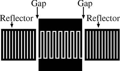
Figure 8.1 The basic configuration of an IDT electrode in a SAW resonator 5)
Periodic signals, generated by applying a voltage to an Inter-Digital Transducer (IDT) formed on a piezoelectric substrate (LN or LT substrate), are transmitted on the surface as SAWs.
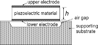
Figure 8.2 The basic configuration of a FBAR 5)
A piezoelectric thin film is supported by very thin dielectric thin films and metallic electrodes, and the Si substrate supporting them has void spaces. Therefore, the piezoelectric thin film can resonate at a frequency higher than the SAW without being affected by the Si substrate. In addition, due to further increase in transferred data volume, a Solid-Mounted Resonator (SMR) structure compatible with the Sub-6 bandwidth is provided. Figure 8.3 shows its structure. All these radio frequency components are formed through PVD. FBAR is a resonator utilizing the BAWs that are transmitted in the thickness direction in the frequency, and Figure 8.2 shows its conceptual diagram.
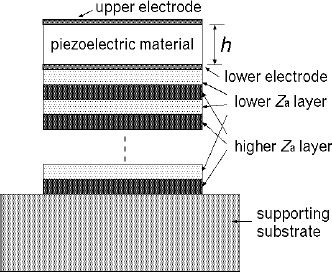
Figure 8.3 The basic configuration of a SMR 5)
8.2.6 Photovoltaic cell
In amorphous silicon films that can be formed by decomposing silane gas (SiH4) through plasma CVD, electrons that are not chemically bonded (dangling bonds) are terminated with hydrogen. Therefore, p-type and n-type amorphous silicon, which could not be made through other film forming methods (such as vacuum deposition and sputtering), can be made. This achieved the practical realization of thin film photovoltaic cells using amorphous silicon and reduction in photovoltaic cell costs.
8.3 Mechanical performance
8.3.1 High hardness and wear resistance
For the purpose of extending the service life of cutting tools, such as drills and turning tools, or various types of molds/dies by forming a rigid film on their surfaces, both PVD and CVD are actively used. Most of the films used in PVD are nitride, carbonized, or carbonitride films of Ti or Cr. The film types are selected according to the materials of the tools and molds/dies, as well as how force is applied to them when they are in use, and multi-layer films are used in some cases. As a result, their service life becomes approximately three to six times longer. The ion plating method is mainly used to form the thin films, and in particular, the cathode arc method and the method using a hollow cathode type plasma gun are commonly employed.
The three main film types that are also used in CVD are TiC, TiN, and Al2O3, which are produced in the following chemical reactions:
- TiCl4+CH4→TiC+4HCl
- TiCl4+1/2N2+2H2→TiN+4HCl
- 2AlCl3+3/2CO2+H2→Al2O3+3CO+6HCl
Although these films are generally formed through thermal CVD at a temperature of approximately 1,000°C, plasma CVD enables the formation of these films at a temperature of approximately 500°C. In addition, a multi-layer film configuration is employed when needed.
Furthermore, Diamond-Like Carbon (DLC) was put to practical use through CVD in this field.
8.4 Chemical application performance
8.4.1 Corrosion resistance
To prevent metals from rusting, wet surface treatment technologies such as coating and plating have generally been used. In recent years, thin films formed through PVD and CVD, which can achieve higher durability and corrosion resistance, were put into consideration.
Both PVD and CVD enable the formation of thin films, which cannot be formed through wet surface treatments, on various types of substrates.
PVD, which employs ion plating and sputtering, is mainly used for substrates whose heat resistance is not so high. In addition, CVD has an advantage in forming films on substrates with a complex shape.
8.4.2 Barrier property
Plastic films are used for food wrappers. For food preservation, the oxygen and ultraviolet barrier properties are particularly required. Therefore, plastic films on which a thin film is formed through PVD are used. Generally, Al films are used for opaque films, and SiOx (1 < x < 2) films are used for transparent films. These films are formed with roll coaters for vacuum deposition and sputtering.
8.5 References
- Edited by Japan Vacuum Industry Association: Learning the Elements of Vacuum Technology, Kogyo Chosakai Publishing Co., Ltd. (1999)
- Edited by the Surface Finishing Society of Japan, The Basics and Application of PVD and CVD Films, Maki Shoten (1994)
- Edited by Complete Guide to Surface Modification Technology Editorial Committee: Complete Guide to Surface Modification Technology, page 191, Industrial Technology Service Center (1993)
- Hitoshi Habuka, Advancement of Atomic Layer Deposition in Semiconductor Materials Manufacturing Process: Cleaning Technology for Thin Film Formation Reactor, J. Vac. Soc. Jpn. Vol. 54, No. 2 (2011)
- Kenya Hashimoto, Functional Radio Frequency Acoustic Wave Devices: Current Status and Future Prospects, IEICE Fundamentals Review Vol. 4, No. 3 (2011)
- H. Ieki, et al., SAW Resonator Using Epitaxially Grown Al Electrodes, Jpn. J. Appl. Phys., Vol. 30 (1991)
- O.Nakagawara et al. , Epitaxially grown aluminum films with titanium intermediate layer on y rotated Y2X LiNbO3 piezoelectric single crystal substrate, Journal of Crystal Growth 249 97-501(2003)
9. Examples and applications of films formed with Shincron’s film forming systems