

5. Various film deposition technologies based on the Physical Vapor Deposition (PVD) method
PVD is a method for forming thin films by vaporizing thin film materials in some way in a vacuum container and depositing them onto a substrate placed nearby. Various technologies are used according to the applications, and they are classified into evaporation group and sputtering group in terms of the thin film material vaporization method, as shown in Table5.1.
Table 5.1 The categories of major PVD technologies
| Evaporation group | Sputtering group |
|---|---|
| Vacuum Deposition | Diode Sputtering(Conventional Sputtering) |
| Ion beam Assisted Deposition (IAD) | Magnetron Sputtering |
| Ion Plating | Reactive Sputtering |
| Molecular Beam Epitaxy (MBE) | Radical Assisted Sputtering |
| Ion Beam Sputtering (IBS) | |
| ECR Sputtering |
5.1 Evaporation group
The technologies in the evaporation group heat thin film materials to evaporate them and then precipitate and solidify them on a substrate surface at a temperature lower than the evaporation temperature to form thin films.
As evaporation sources, 1. resistance heating, 2. electron beam heating, 3. high-frequency induction heating, and 4. laser beam heating are used.
Among them, electron beam heating is used the most, because it can evaporate almost all materials other than high-melting-point metals. Resistance heating is a method that heats vaporized materials by directly energizing high-melting-point metals such as tungsten, tantalum, and molybdenum. The high-melting point metals are in filament-like or boat-like shapes so that the materials used to form the thin film can be hung or placed on them to heat and evaporate such materials.
In addition, there is also a method, such as Knudsen Cell (K-Cell), where materials are put in a crucible, which is made of ceramic and other metals such as high-purity carbon and PBN, wound with a heater around the outside, and then heated to form films. This method is used for the formation of films using materials whose evaporation temperature is relatively low, such as organic substances, metals including aluminum, gold, silver, and copper, and compounds.
High-frequency induction heating is used for large-volume evaporation sources for aluminum, and laser beam heating is characterized by no change in the ratio of components of evaporation materials and formed films in the formation of compound films.
5.1.1 Vacuum Deposition
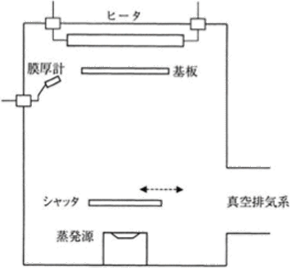
Figure 5.1 The concept of vacuum deposition 18)
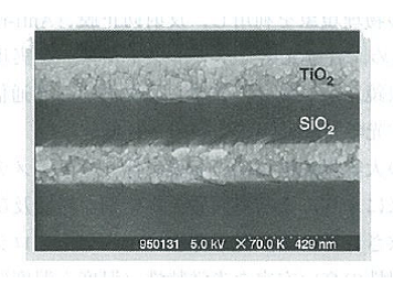
Figure 5.2 A cross-sectional SEM image of a vacuum-deposited multi-layer film 2)
As Figure 5.1 shows, vacuum deposition is performed with an evaporation source and a substrate placed in a vacuum container. In general, the gas is exhausted from the vacuum container until the pressure inside it decreases to approximately 10-4 Pa, and a film is formed under the pressure between 10-2 and 10-4 Pa. In this case, as the mean free path is between several tens of centimeters and several tens of meters, the thin film materials evaporated from the evaporation source reach the substrate without colliding with the residual gas. In the vacuum deposition, the evaporation particle energy is only approximately 0.1 – 0.3 eV, which consists of the energy equivalent to the evaporation source temperature and the thermal energy generated by heating the substrate. Therefore, there is an advantage that substrates become less damaged and thin films are less likely to contain impurities. On the other hand, however, thin films tend to be porous, have low densities and refractive indexes, and have insufficient film strength. Figure 5.2 shows a SEM (Scanning Electron Microscope) image of the cross-section area of a TiO2/SiO2 laminated film formed under the best available conditions.
5.1.2 Ion-beam Assisted Deposition (IAD)
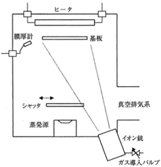
Figure 5.3 The outline of IAD 18)
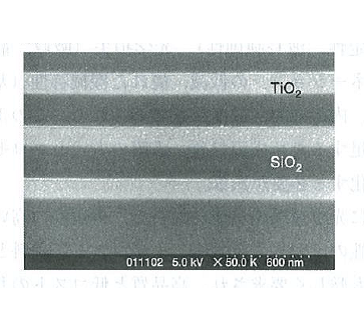
Figure 5.4 A cross-sectional SEM image of a multi-layer film formed through IAD 2)
The IAD method was developed by adding aggressive irradiation of ions on substrates to the forementioned vacuum deposition method, and was improved and generalized for the formation of optical thin films. The features of the IAD method are described below, focusing on its optical thin film formation technology.1)2)
Figure 5.3 shows the outline of the IAD method. A film forming system based on the IAD method has an electron gun for an evaporation source, a substrate holder with a substrate rotation mechanism, a substrate heater, an optical thin film thickness control system, and an ion source in its vacuum chamber.
The features of the formation of optical thin films using the IAD method are as described below.
- The plasma generation process is spatially separated from the film forming process
– Enables the reduction of contamination
– Enables the formation of highly-reproducible thin films in a stable process, because there is less change in the atmosphere during the film forming process
– Enables the film forming process to be conducted at a relatively low pressure - Enables independent control of ion energy and ionic current density
– Enables the acceleration of the film forming rate by increasing the current density
– Enables the formation of thin films with high film density and less optical scattering
– Enables an easy change of thin film properties based on the process conditions - Enables the formation of large and uniform films
Although the IAD method enables the enhancement and improvement of various characteristics of thin films such as optical characteristics and structure, it is essential to set the vacuum deposition parameters (film forming pressure and rate, and substrate temperature) and the IAD-specific parameters (ion type, current, and energy) optimally, in order to achieve the required characteristics of optical thin films. In the case of the IAD method, the conditions need to be considered based on the ratio of the film forming deposition molecules (atoms) and the ions that reach a substrate γ3).
The ratio of the deposition molecules (atoms) and ions that reach a substrate γ is defined as follows:

NA: Avogadro constant, RM: Deposition rate [Å/sec], M: Molecular weight of deposition material, DM: Density of deposition material [g/m3], Ji: Ion current density [μA/cm2]
In addition to the ratio of the deposition particles and the ions that reach a substrate, the type, energy, and neutralization efficiency of the ion particles are also important parameters for the IAD process. As a lot of oxide materials are used for forming optical thin films, oxygen ions are generally irradiated. The ion source used for the IAD can independently control the ion irradiation energy and ion current density. If the ion energy is too high during film formation, the formed film is sputtered or an oxygen loss occurs. Therefore, it is necessary to optimize the ion energy and current density conditions through thin film materials. In order to express ion condition parameters in a concentrated way, the product of a measured value of ion current density on a substrate dome and the acceleration voltage representing the ion energy is defined as ion power density.
Based on the above, taking Ta2O5, TiO2, and SiO2 that are commonly used for optical thin films as examples, the relationship between the optical constants (refractive index and attenuation coefficient) or microstructure of the thin film and the ion current power density is investigated and the result is described below.
- Ta2O5
Ta2O5 is a very stable oxide and is widely used as a deposition material with low absorptivity and a high refractive rate in the 0.35 to 8 μm range. Figure 5.5 shows the relationship among the ion power density, the refractive index, and attenuation coefficient of a Ta2O5 thin film. In the formation of the Ta2O5 thin film, the substrate temperature and film forming rate were set to 150°C and 0.6 nm/s, respectively, and the acceleration voltage was varied in the range up to 1,000 V.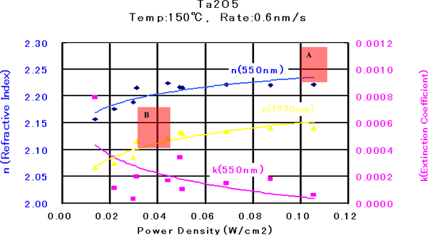
Figure 5.5 The relationship between the optical constants (refractive index and attenuation coefficient) of Ta2O5 thin film and the ion power density 2)
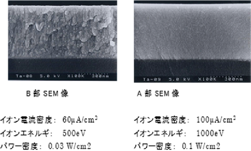
Figure 5.6 Cross-sectional SEM images of Ta2O5 single-layer films formed under different conditions 2)
There is a tendency that the higher the power density is, the higher the refractive index becomes and the lower the extinction coefficient becomes. When the power density becomes 0.05 W/cm2 or higher, the refractive index becomes stable at approximately 2.22 (@ 550 nm). In this case, the extinction coefficient becomes 1 x 10⁻⁴ level. Figure 6 shows the cross-sectional SEM images of Ta2O5 single-layer films formed at the power density of 0.03 W/cm2 (Section A) and 0.1 W/cm2 (Section B). It can be found that Section B shows a columnar structure while Section A shows a dense structure. - TiO2
TiO2 is generally used as a high refractive index material at optical thin film production sites, because its refractive index is high (approximately 2.2 – 2.5) and its transmittance is also high and ranges from the visible light to infrared regions. However, TiO2 tends to cause optical loss (scattering and absorption), and it used to be very difficult to form high density (wavelength shift-less) films. When forming TiO2 thin films using the IAD method, not only is absorption likely to occur due to oxygen defect, but also scattering is likely to occur because of the formation of a crystal structure of anatase and rutile. Therefore, it is important to optimize the ion energy and substrate temperature.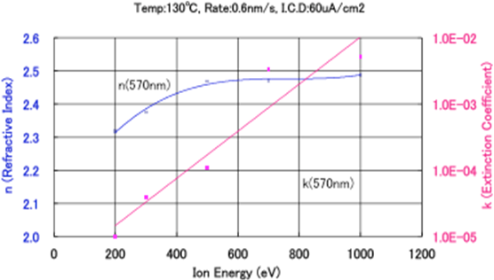
Figure 5.7 The relationship between the optical constants of TiO2 thin films and the ion energy when the IAD method is used 2)
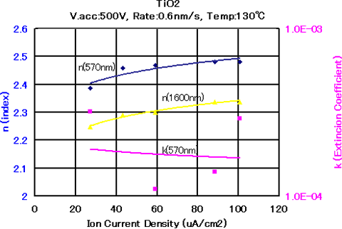
Figure 5.8 The relationship between the optical constants of TiO2 thin films and the ion current density when the IAD method is used 2)
Figures 5.7 and 5.8 show the relationship between the refractive index and the extinction coefficient in the formation of TiO2 films, when the substrate temperature and film forming rate were fixed at 130℃ and 0.6 nm/s, respectively, and the acceleration voltage and current density were independently varied as film forming parameters. As Figure 7 shows, if the acceleration voltage becomes 500 V or higher when the ion current density is 60 μA/cm2, the refractive index becomes 2.46 – 2.47. On the other hand, Figure 5.8 shows that the refractive index of the thin film increases as the ion current density increases, when the acceleration voltage is fixed at 500 V and the ion current density is changed from 30 to 100 μA/cm2. - SiO2
SiO2 is a mechanically and chemically stable substance, has a wide wavelength range, and is transparent. Therefore, it is essential as a low refractive index material for the optical multi-layer film configuration. As is the case with Ta2O5, this substance also enables stable formation of films at an acceleration voltage of up to 1,000 V. Figure 5.9 shows the relationship among the ion power density, refractive index, and attenuation coefficient when the film forming rate is fixed at 1 nm/s at the substrate temperature of 120℃. As the ion power density increases, the refractive index of the SiO2 thin film also increases. When the ion power density becomes 0.04 w/cm2 or higher, the refractive index increases to 1.46 or higher, which enables the formation of dense thin films in a relatively wide process range.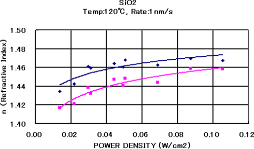
Figure 5.9 The optical constants of SiO2 when the IAD method is used 2)
5.1.3 Ion Plating
Beginning with the method utilizing a direct-current discharge that was presented by D. M. Mattox in 19644), various film forming methods were researched and developed based on this technology. In the Mattox method, several kilovolts of negative voltage is applied to a substrate, and a film is formed under a pressure of several pascals. The ions of the introduced argon gas and evaporation particles collide with the substrate after being accelerated by the potential difference between the substrate and the cathode dark space near the substrate. The characteristic of this method is that using this energy enables the formation of thin films with strong adhesion. Furthermore, as this method achieves superior throwing power because of the formation of films under a pressure with a short mean free path, it is utilized for forming films on soft metals such as solid lubricant for the bearings employed in aerospace systems. Afterwards, as shown in Figure 5.10, various methods were developed that employ some sort of ionization means between an evaporation source and a substrate, and the applications have been expanded. Major ionization means include the followings:
- A probe to which a positive voltage is applied is placed directly above an electron gun evaporation source, and the reflection and secondary electrons are accelerated to be used for ionization5)
- A high-frequency discharge is used to form films in an argon or reactive gas atmosphere of the 10-2 Pa level6)
- A Hollow Cathode Discharge (HCD) type low-voltage and large-current electron gun (plasma gun) is utilized for ionization and evaporation7)
In ion plating, a negative pressure or high-frequency wave (in the case of insulating films) is applied to a substrate, and the ions are irradiated to the substrate. In addition, as the atmosphere is active, introducing a reactive gas such as oxygen, nitrogen, and acetylene enables the formation of oxide, nitride, and carbide films. In general, as ion-plated films are highly adhesive, this method enables the formation of high-density thin films. Therefore, it is mainly used for the formation of films requiring high rigidity, high lubricity, and abrasion-resistance for cutting tools and molds/dies, TiN and CrN films as nitride films, TiC and Cr3C2 films as carbonized films, and TiCN films as carbonitride films.
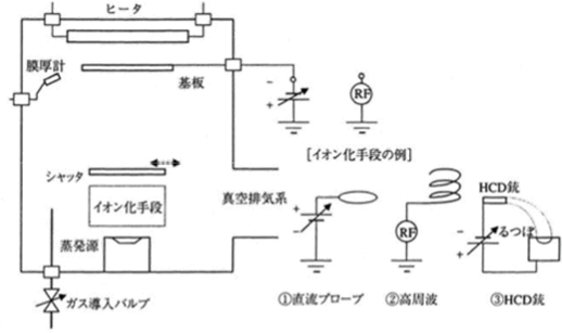
Figure 5.10 The conceptual diagram of the ion plating 18)
5.1.4 Molecular Beam Epitaxy (MBE)
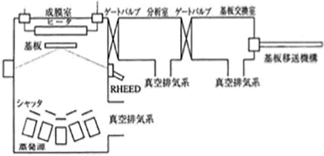
Figure 5.11 The configuration of an MBE system 18)
Figure 5.11 shows the configuration of an MBE system. Using the MBE enables the utilization of molecular beams that are almost in the same direction. As an evaporation source, a Knudsen Cell (K Cell) consisting of a resistance heating crucible equipped with an orifice on its vapor outlet is used. The evaporation source is temperature-controlled in a precise manner, and the films are formed on an atomic monolayer basis while being observed through Reflection High Energy Electron Diffraction (RHEED). Therefore, as the influence of the residual gas in the film forming chamber is significant, the films need to be formed in an ultrahigh vacuum of 10-7 – 10-9 Pa. This system is mainly used for the formation of semiconductor single-crystal films, and also enables impurity doping. In addition, superlattices (artificial lattice structures) can also be formed with this system. The method that utilizes a laser as an evaporation source is used for the formation of oxide superconducting thin films, and is called Laser Ablation. In this system, a substrate exchange chamber and an analysis chamber are also connected in addition to a film forming chamber, and each chamber is separated by gate valves. The substrates are also transferred by a manipulator.
5.2 Sputtering group
Sputtering method refers to depositing target material particles, released into the gas phase through a momentum exchange caused by the collision of high energy particles with the target material in a vacuum, on a substrate. Figure 5.12 shows the sputtering phenomenon in a schematic manner.8)9)
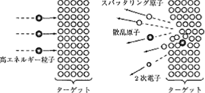
Figure 5.12 The schematic diagram of the sputtering phenomenon 9)
A plasma is used to obtain particles whose energy is high enough for causing sputtering. The features of the sputtering method are as described below.
- Enables the formation of thin films which can adhere strongly to substrates even at a low temperature as well as have a dense structure
- Enables the formation of uniform films on large-area substrates
- Realizes long target life and is suitable for mass production
- Superior reproducibility and stability
- Enables the reduction of system capacity, because of enabling the shortening of the distance between a target and a substrate
5.2.1 Sputtering rate and energy
Sputtering rate refers to the number of atoms ejected into the gas phase per incident particle as a result of sputtering. Figure 5.13 shows the energy dependency of the case where Ne+, Ar+, Kr+, and Xe+ are incident upon a silicon target.9)10)
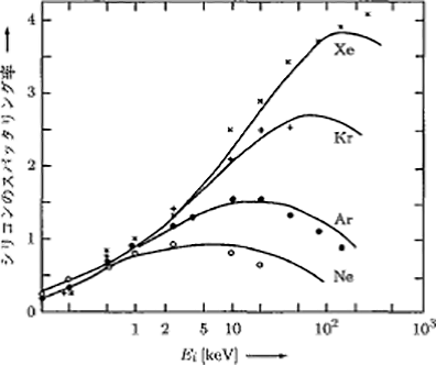
Figure 5.13 The dependency of the sputtering rate of Si on the incident energy and gas type 9)
Figure 5.14 shows the sputtering rates of the case where Ar+ with energy of 400 eV is incident upon various types of target materials.9)11) The sputtering rate changes periodically and shows the largest values with respect to Al, Cu, Ag, and Au. On the contrary, it shows small values with respect to C, Ti, Zr, Ta, and so on.
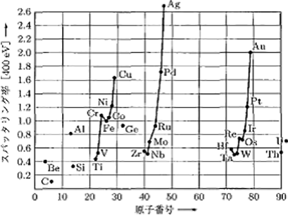
Figure 5.14 The sputtering rates of the case where Ar+ with energy of 400 eV is incident upon various types of target materials 9)
Figure 5.15 shows the energy distribution of the atoms released into the gas phase through sputtering. Compared to the energy of deposited particles of 0.1 – 0.3 eV in the case of deposition, it is found that the energy achieves a peak at around 2 eV in the case of sputtering.
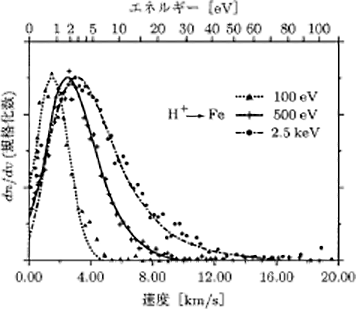
Figure 5.15 The distribution of energy of sputtered particles 9)
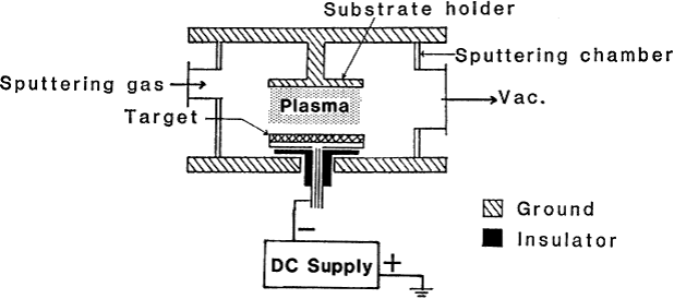
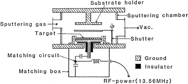
5.2.2 Diode Sputtering (Conventional Sputtering)
Diode sputtering is a method that employs the simplest system configuration. As Figure 5.16 shows, a substrate is placed opposite to a target in a parallel manner, and several kilovolts of negative direct-current (high-frequency) voltage is applied to the target in an argon gas atmosphere of between several and several tens of pascals to cause an electric discharge. Its characteristics are as follows:
- The deposition rate is low, because the discharge voltage is high but the current density is low
- Sputtered particles collide with a discharge gas and scatter because of high discharge voltage and then lose their energy
In addition, the following descriptions are applicable depending on the type of the power source connected:
- DC Magnetron Sputtering that uses a DC power source and forms films on conductive materials such as metals
- RF Magnetron Sputtering that uses an RF power source and forms films on insulating materials and so on
(a) DC Magnetron Sputtering
(b) RF Magnetron Sputtering
Figure 5.16 The outline of a sputtering power circuit 13)
Since the development of the magnetron sputtering method that compensates for these shortcomings, these sputtering methods have been little used in production.
5.2.3 Magnetron Sputtering
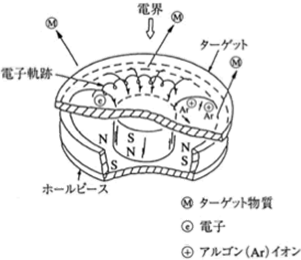
Figure 5.17 Magnetron cathode 18)
The magnetron cathode, as shown in Figure 5.17, improved the shortcomings of the diode sputtering. It utilizes the leakage magnetic field on a target surface, with a magnet placed at the back side of the target. This magnetic field makes electrons move around in the magnetic field while drawing toroidal curves near the target surface. Because of this, strong plasma is generated along the orbits of the electrons and this area is intensively sputtered, resulting in an increase in the sputtering rate of 10 – 100 times. The magnetron sputtering is used differently depending on the power source connected.
5.2.4 Reactive Sputtering
Reactive sputtering is a method where metallic atoms are sputtered from a metallic target, and then reacted with an active gas such as O2 and N2 to form a thin compound film on a substrate.
The characteristics of reactive sputtering are as follows:
- The film forming rate is low, compared to the deposition and chemical vapor deposition methods
- A hysteresis phenomenon occurs against gas introduction
If the reactive gas is increased or decreased while keeping a constant discharge current, the hysteresis phenomenon as shown in Figure 5.18 occurs. Therefore, control of the film forming rate becomes complicated.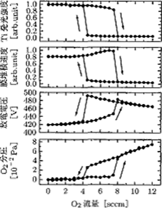
Figure 5.18 The formation of a hysteresis under the reactive sputtering method 9)
- An abnormal electric discharge on the target surface (Refer to Figure 5.19.)
Under the reactive sputtering method, the erosion region of the target is conductive because its metallic surface is constantly maintained through sputtering. On the other hand, however, insulators deposit on the non-erosion region because it is not sputtered. The surfaces of insulators are charged positively because of the deposition of ions. If the potential difference between an insulator surface and a metallic cathode surface exceeds a certain limit, an insulation breakdown occurs. This phenomenon is a big problem for the reactive sputtering method, and it can be solved by the pulse sputtering method or the RAS method to be hereinafter described.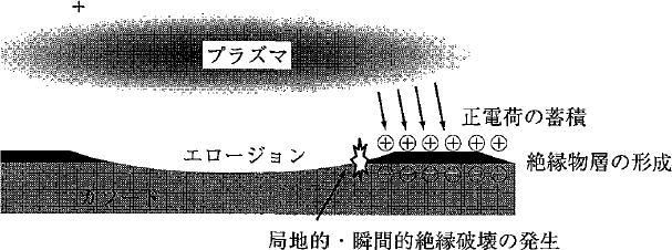
Figure 5.19 A model of an abnormal electric discharge associated with the formation of insulator deposits 9)
- Anode disappearance15)
In reactive sputtering, the targets serve as cathodes and the vacuum container wall and so on serve as anodes (earths). In both cases, if the insulators start to deposit on an anode surface as a result of reactive sputtering, there are cases where the anode becomes unworkable as an electrode and the electrons’ destination is lost. This phenomenon is called anode disappearance. It causes a variation in and instability of the discharge state and affects the deposition rate and structure of thin films significantly.
5.2.5 Radical Assisted Sputtering (RAS) method
The sputtering process is an active energic process because the kinetic energy of adhesive particles is several electron volts, which is an order of magnitude higher than that of the vacuum deposition method. Therefore, a dense microstructure can be obtained. However, in the case of optical thin films that are highly transparent dielectric thin films, it had been impossible to form high quality optical thin films using the conventional reactive sputtering method because of the problems of low film forming rate, hysteresis against gas introduction, abnormal electric discharge near the targets, and anode disappearance as described earlier. The RAS method is a film forming method that solved such problems and is currently used in the mass production of a wide variety of optical thin films.
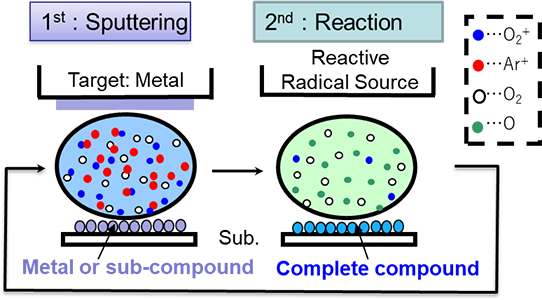
Figure 5.20 The figure of the principle of the RAS method 16)
Figure 5.20 shows the principle of the RAS method. Under the standard reactive sputtering method, the sputtering and reaction processes are performed in one region. On the other hand, under the RAS method, these regions are separated spatially and electrically, enabling independent control.
The processes are described in detail below, taking the formation of an oxide film as an example.
Employing a dual cathode to maintain a stable anode, and the film forming process where metallic or metallic incomplete oxide films is repeated with a complete oxidation process using a strong oxygen radical source, high-density oxides can be laminated at a high speed and low temperature. Figure 5.21 shows the schematic diagram of a RAS system. The RAS system employs a load lock system for preventing the oxidation of the cathode due to substrate transfer and realizing a stable film formation process.
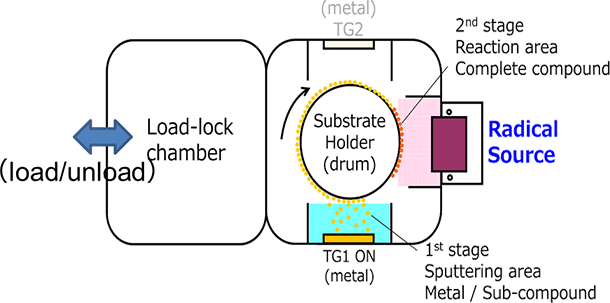
Figure 5.21 The schematic diagram of a RAS system 17)
5.2.6 Ion Beam Sputtering
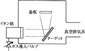
Figure 5.22 Ion Beam Sputtering 18)
As Figure 5.22 shows, the gas ions are irradiated onto a target with an ion gun to perform sputtering. As an electric discharge does not need to be generated in the film forming chamber, it is possible to form films in a high vacuum. Therefore, this method enables the formation of high precision optical multi-layer films that cause less scattering.
5.2.7 ECR Sputtering
An Electron Cyclotron Resonance (ECR) condition is created using the microwave of 2.45 GHz and the magnetic field of 8.75 x 10⁻² T to generate a strong electric discharge. With a target placed between this plasma and a substrate, biasing it negatively causes sputtering to form films.
5.3 References
- Shigeharu Matsumoto, Development of an Ion Source Suitable for the Formation of Optical Thin Films, Vacuum Journal, January, No. 116 (2008)
- Jiang Yousong, Shigeharu Matsumoto, Deposition Technology and Its Expansion, OPTRONICS, No. 10 (2013)
- Qi Tang, Sigetaro Ogura, Kazuo Kikuchi, Nobuyuki Higashi, Optical and Structural Properties of Tantalum Pentoxide Thin Films by Ion Assisted Deposition Method with Radio Frequency Ion Source, The Review of Laser Engineering, Volume 42, Issue 3 (1996)
- D. M. Mattox, Electrochem. Tech., Sept. – Oct. 2, 295 (1964)
- R. F. Bunshah and A. C. Raghuram, J. Vac. Sci. Tech., 9, 1385 (1972)
- Yoichi Murayama, Masayuki Matsumoto, Kunihiro Kashiwagi, Applied Physics, 43, 687 (1974)
- C. T. Wan, D. L. Chambers and D. C. Carmichael, J. Vac. Sci. Tech., 8, No. 6, VM 99 (1971)
- Akira Kinbara, Sputtering Phenomenon – Basics and Application to Thin Film and Coating Technologies, University of Tokyo Press (1984)
- Eiji Kusano, The First Thin Film Forming Technology (Second Edition), Morikita Publishing (2012)
- P. C. Zalm, J. Appl. Phys. 54, 2660 (1983)
- N. Legreid, G. K. Wehner, J. Appl. Phys. 32, 365 (1961)
- H. L. Bay, Nucl. Inst. Methods. in Phys. Res. Sect. B, 18, 1-6, 430-445 (1986)
- Makoto Kitabatake, Kiyotaka Wasa, Thin Films Formed through Sputtering, Surface Chemistry, Vol. 5, No. 4 (1984)
- E. Kusano, J. Appl. Phys. 70, 7089 (1991)
- Akira Kinbara, Eiji Kusano, Masahiko Sakamoto: Historical Transition in Sputtering Method, J. Vac. Soc. Jpn., Vol. 46, No. 10 (2003)
- Ekishu Nagae, Shincron’s Sputtering Film Forming System for Optical Muti-Layer Films, Vacuum Technology Outlook 2006, Separate Volume of Electric Journal (2006)
- Shincron Co., Ltd., RAS-1100 Catalogue
- Edited by Japan Vacuum Industry Association: Learning the Elements of Vacuum Technology, Kogyo Chosakai Publishing Co., Ltd. (1999)